
Summary:
It is shown that the shape of the transfer function and of the SNR of the internal ADC of the STM32H7 vs. frequency of the applied signal can be explained with a very simple simulation model up to quite high signal frequencies. The PLL that drives the ADC and also the internal switch that connects the input signal to the sampling capacitor is very jittery. The simulations show a good fit with the measured data for RMS jitter values of around 100 ps and switch resistances of about 2 kOhm.
The former blog entry Part II already deals with signal-to-noise-ratios of the 16-bit-ADC inside of the STM32H743ZI (old revision Y). The diagram shown there in the summary shows measurements of the signal amplitudes and the noise floors of FFTs taken from H7-ADC data for quite a range of signal frequencies between 0.5 MHz and more than 1000 MHz. The ADC signal input has been connected to a laboratory RF generator in two different ways, as described in Part I of the blog entry.
The results show an almost negligible difference between a single-ended and a differential connection method in terms of bandwidth and noise. What is striking about the measurement results, however, is that the noise floor increases by 6 dB per octave from just 0.5 MHz, the lowest signal frequency used for the measurements. The reason for this is investigated in this blog entry.
The noise of an ADC when digitizing a signal should consist of at least two components: a component that is independent of the signal frequency and that describes the amplitude noise of the ADC (quantization noise, thermal noise), and a component that is proportional to the signal frequency and is determined by the uncertainty of the sampling time. This uncertainty in the sampling time is caused, for example, by the phase noise of the clock oscillator that drives the ADC, but also by the additional phase noise of other components in the signal path that determine the sampling time of the sample. More information can be found here or here and in many other papers.
When an ADC does not show a constant noise level at low signal frequencies and the noise curve rises proportional to the frequency even for very low signal frequencies, the noise of the ADC may be determined mainly by the ADC aperture jitter, or by the sampling clock jitter, or by both.
In order to get a rough number for this jitter, I wrote a program that simulates the measurements by using a very simple simulation model.
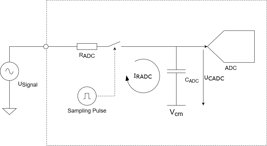
I assumed an ideal 16-bit-ADC, i.e. an ideal ADC with zero DNL and zero additional amplitude noise. The python script aperturejitter.py simulates a signal with exactly the same amplitude as it was used in the actual measurements. In order to simulate the time jitter, a normally distributed random number was added at the beginning and at the end of each sampling pulse. The standard deviation of this random number corresponds to the rms value of a specific time jitter. After the closure of the switch the campling capacitor CADC gets connected to the signal source via the switch resistance RADC. The sampling capacitor now gets charged with a current proportional to the difference between the signal voltage and the voltage across the capacitor. The sampling interval is divided into a number of small steps and the capacitor voltage is calculated at the end of each step before the next iteration step. This way the voltage across the sampling capacitor at the end of the sampling interval can be calculated and the digitized value can be calculated by a simple float-to-uint16-conversion.
The measured transfer function of the ADC has a pole at around 20 MHz, so RADC should about ~2 kOhm with CADC = 4 pF as stated in the datasheet. The simulated curve of the transfer function („max in dB(model)“) shows a good fit with these simulation parameters. A good fit to the measured SNR data („max/noise_floor in dB(model)“) has been achieved with a rms time jitter value of 100 ps.
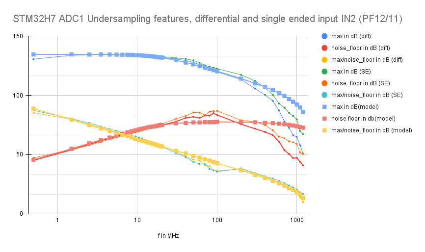
Even the agreement with the measured values of the noise floor („noise floor in dB(model)“) is quite good at frequencies up to well above several 10 MHz. At higher frequencies, the match is less good. Possible explanations for this could be additional high frequency poles at about 200 MHz and 700 MHz, but this is only speculation. I could not find further information about this in the ST documents.
Possible improvements:
The reference manual and the data sheet of the STM32H7 mention that the ADC clock could also be derived from the AHB clock (rev Y) or from the system clock (rev V) without using a PLL output. This could improve the clock jitter but also reduces the flexibility of the ADC. I’ll give it a try maybe…