
TI’s new family of SAR-ADCs with integrated DDCs could be a game changer for building SDRs for HAM radio operators.
Why?
Because these ADCs do not only contain an NCO and a complex digital IQ downmixer, they also integrate a decimation stage and an output formatter that potentially allows a direct connection to an MCU!
And they are rather inexpensive, with prices far below 100.- €, see ADC3643 or ADC3660, even in single quantities.
That means that you probably can build a SDR receiver with a similar quality as the HPSDR or Pavel Demins port to the Red Pitaya without having to resort to FPGAs.
Take a look at the datasheet of the ADC3660:
- 2 ADC-Channels, each running at a sampling rate of up to 65 Msps. This should be enough to cover every amateur radio band including the 10 m band
- 900 MHz analog bandwith. Enough to cover even the 70 cm band by bandpass-sampling techniques. Very low aperture jitter, which is also important for high quality undersampling techniques
- integrated 32-bit-NCO. This should give us a frequency resolution of 65 Msps/2^32 = 15 Millihertz. Far better than we ever need for amateur radio purposes
- Very low power. Only 71mW per channel. Very interesting for battery operation
- Serial CMOS outputs. Handy for connecting to a MCU
- Maximum decimation rate of 32. With 2 x 16 bits of IQ-data output every 32th clock cycle of the sampling clock, the output data rate will be 65 Msps. This should be well within the range of SPI peripherals of modern MCUs.
- The ouput formatter can be programmed for 1-wire serialization, which means that the IQ data is output on a single lane
- The data clock signal is usually of DDR type, which means that both edges of the clock signal are used for clocking out the data. This is unfavorable for a connection to an MCU. Fortunately, the TI people have also built-in an SDR clocking option, which can be activated by setting bit 3 of register 0x1F
So far, so good.
The only downside of the offered output formats of the ADC3660 is that none of the available formats described in the datasheet are suited for a directed connection to an MCU.
The FCLK signal that is offered by the ADC3660 resembles the LeftRightClock-Signal of an I²S bus.
Unfortunately, I²S peripherals of MCUs are not made for data rates of 65 Msps. The usual application of these peripherals is to communicate with audio codecs at much lower speeds.
Reading through the reference manuals and application notes of my preferred MCU family STM32H7, I found the following diagram in a presentation of the SPI interface of the H7 family:
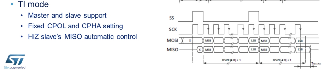
The TI mode seems to be appropriate for transferring a fast serial data stream to my MCU, and my MCU supports exactly this TI mode.
Ironically, TI’s ADC3660 does not support TI’s own mode! At least I couldn’t find any hints of how to program the registers of ADC3660 in order to put out data in TI mode. It could of course be that TI has built in this possibility, but in any case it is not documented in the data sheet.
TI mode
In TI mode, the function of the NSS (Not Slave Select) signal is not to select the SPI slave (which is the MCU in this case).
Instead, the NSS signal is used for signaling the LSB of the transmission. Each time the LSB is sent, the NSS goes high with apparently the same timing as the LSB.
This way the data stream does not have to interrupted between frames and this makes it possible to send an uninterrupted data stream from the ADC to the MCU.
To be continued…