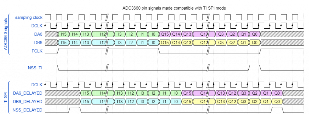
The following timing diagram (that I draw with Wavedrom, a fantastic tool for that purpose) shows in the upper part the output format of the ADC3660 as I understand it from the datasheet:

The signal in the middle („NSS_TI“) shows the NSS signal as it is required for the TI SPI mode.
Unfortunately, it would be quite an effort to produce this signal without any delays. It is possible, but one would need a counter that sets NSS_TI after 31 counts and that is reset by the rising edge of FCLK. The easiest way of realizing such a counter would probably be the use of an FPGA for that, which is exactly what I wanted to avoid.
It is much easier to produce the NSS signal with some delay: One only needs a detector for the rising edge of FCLK.
Of course, in order not to lose synchronization, one then has to delay the data by the same number of clocks as the NSS signal.
The corresponding signals are shown in the lower part of the timing diagram (the signals with the suffix „_DELAYED“)
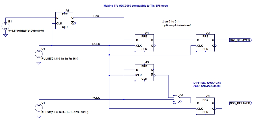
Although that may sound more complicated, it needs only some D-Flip-Flops and only one logic gate:

The AUC logic family is perfectly suited for this purpose: It operates at 1.8 V, which is the same voltage as the IO voltage of the ADC3660, it consumes very low power, is blazingly fast and the output structure is made for 50..65 Ohms transmission lines without the addition of any source resistances.

This is a really neat idea, I see that you made a board on Github, did it work? I’m curious if the STM32H7 actually was able to receive high rate SPI data.
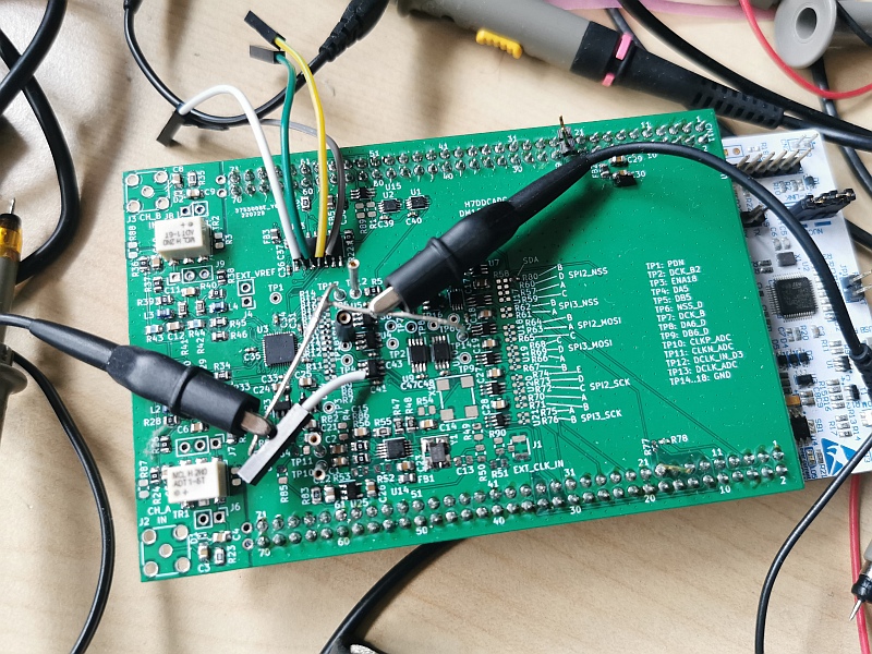
Hi Dave, I have soldered a first prototype:

First measurements show that all the signals look like expected.
Unfortunately, I haven’t found enough time since to really read in the SPI data and do something useful with it. Hold on!