
I have to admit of having had some prejudices about ADCs in microcontrollers.
From my experience, they are slow and noisy of no use for really demanding applications.
Well, the 16-bit ADC peripheral of the STM32H7 of ST Microelectronics may be a real game-changer. It seems to be very flexible and low-noise and really useful for precision applications, too.
In the future, I would like to play around with some undersampling applications, so I wondered what the analog bandwidth of this part is.
The datasheets and reference manuals of ST give no hints on that.
I was curious, so I decided to perform some measurements on this peripheral by myself.
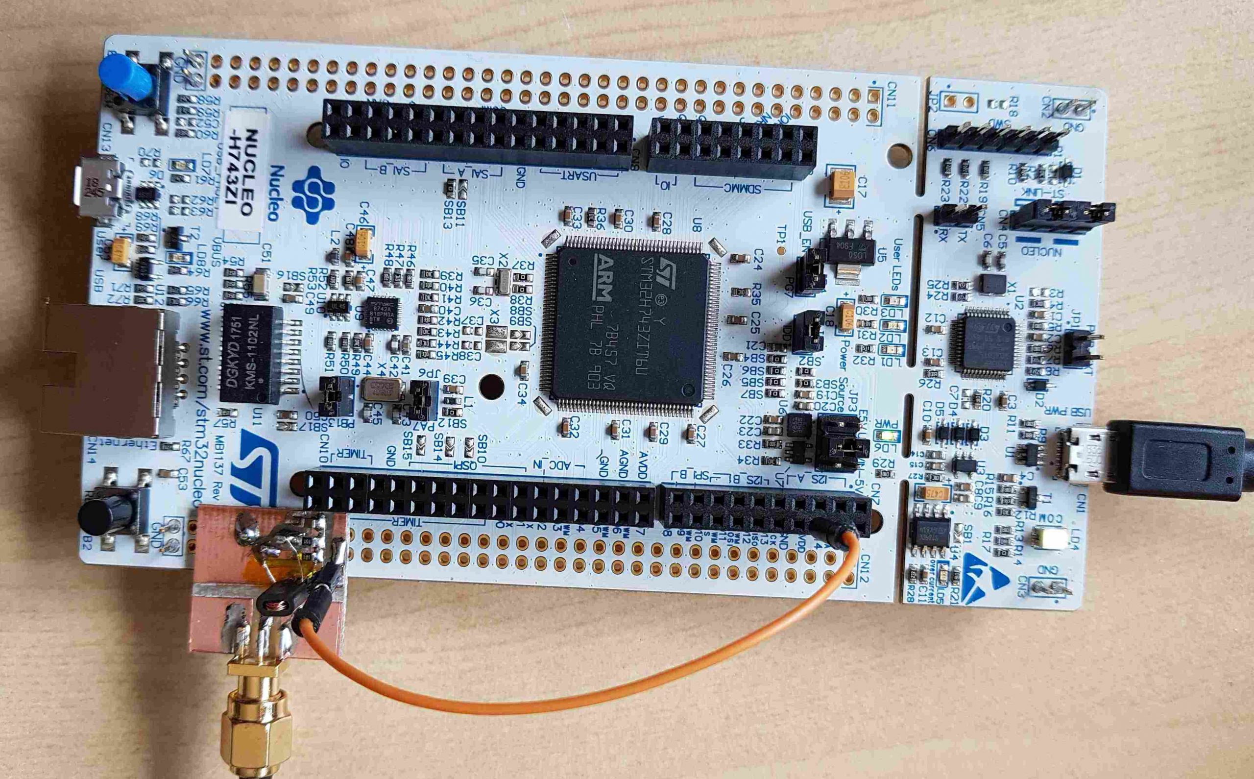
The only hardware I have available for this is some NUCLEO-H743ZI boards that I was able to get at a trade fair a few years ago.
Unfortunately, neither the layout of a NUCLEO-Board nor the package of the STM32H743ZI (a LQFP-144-package) is especially suited for testing the ADC inputs.
In a recent application note (AN5354), ST shows that a UFBGA-176-package should be a much better choice for high-end ADC applications.
Anyway, some NUCLEO boards are all what I have and I have to try my very best with them.
One of the first questions that come to mind is: Which one of the three ADCs and which one of the many possible input pins for each ADC should i choose?
Chapter 2.4 of this application note distinguishes three different types of ADC inputs:
Slow, fast and direct channels
Input signals connected to the different types of channels have to travel across a different number of internal switches until they reach the buried ADC input. Each switch adds its own ON-resistance along this path, which reduces the bandwidth of the input signal.
The inputs with the smallest number of switches are called „direct channels“.
The LQFP-144 package offers only 2 direct channels. Other packages offer up to 4 direct channels.
By reading the STM32H743 datasheet, if found out that the direct channels are called PA0_C, PA1_C, PC2_C and PC3_C.
PA0 and PA1 are connected to ADC1_IN16 (differential input).
PC2 and PC3 are connected to ADC3_IN1 (differential input).
PA1 is already connected to the ETH Phy (by removing SB13 this connection can be interrupted). Using this pin as ADC test input makes only sense if this connection is removed and I did not want to do this.
PC2 and PC3 seem to be more promising. Both PC2 and PC3 are available on the so-called Morpho-connector CN11.
On the other hand, PC2 and PC3 belong to ADC3, and ADC3 lies in the D3 domain, somewhat apart from the other interesting peripherals.
So, what about the fast channels?
By having a look at the minimum sampling times printed in the data sheet, for example 7.37E-08s, 1.14E-07s and 1.72E-07s for a source resistance of 47 Ohms and 16 bit resolution (Table 185 in the datasheet), one can see that the differences between a slow channel and a fast channel are higher than the differences between a fast channel and direct channel. So, maybe it still makes sense to choose a fast channel instead of direct channel?
Anyway, fast channels are available on PF3, PF5, PF7, PF9, PA6, PC4, PB1, PF11 and PF13, tells the data sheet.
PF11 (ADC1_INP2) and PF12 (ADC1_INN2) seem to be quite appropriate and so I chose these two inputs.
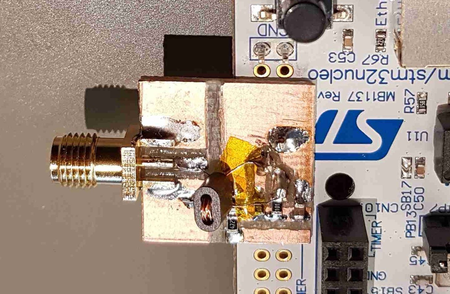
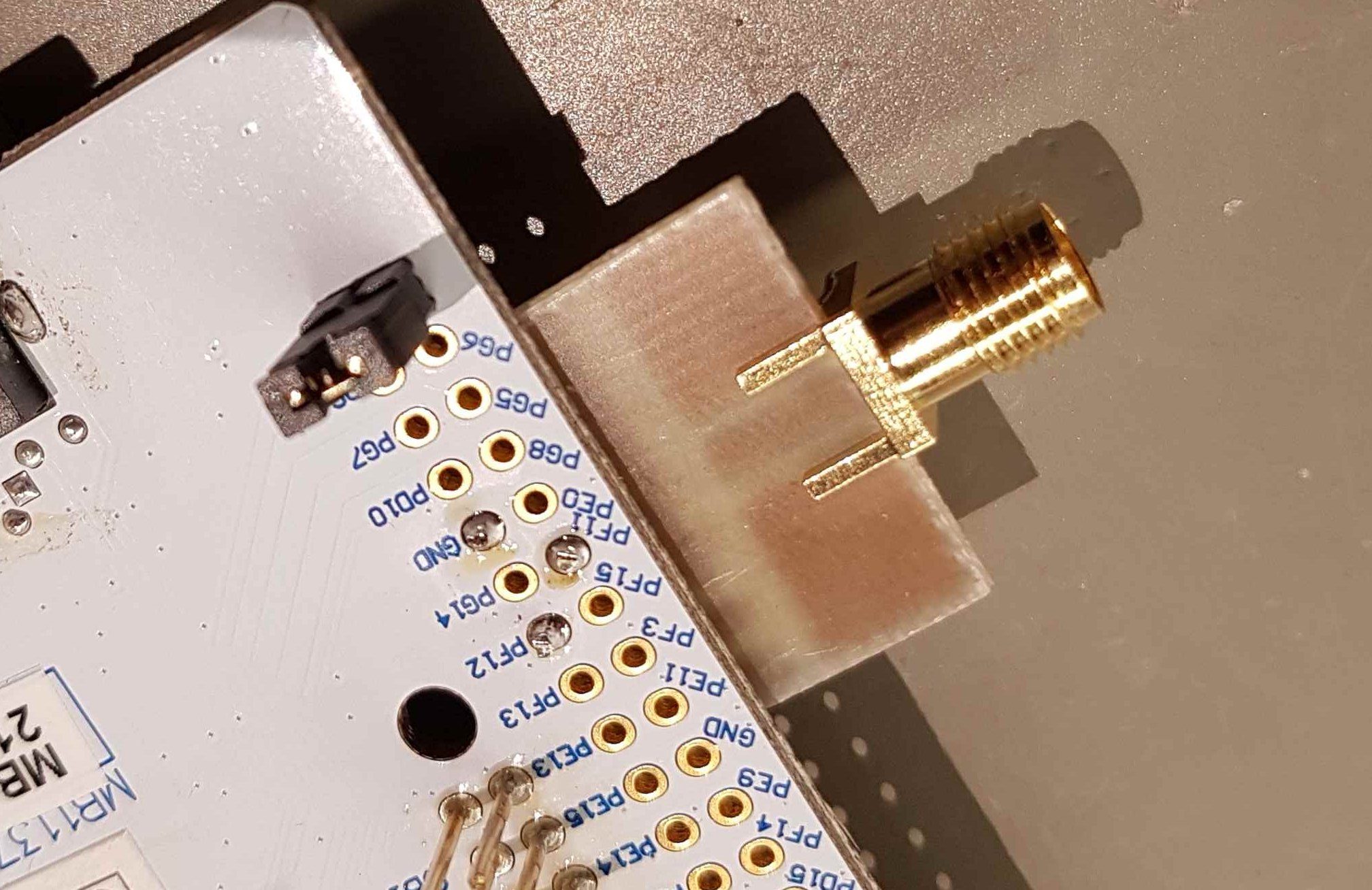
PF11 and PF12 are available on Morpho connector CN12, pin 62 and pin 59. A GND connection is also very close, so maybe these pins are the best choice for feeding RF signals to the ADC.
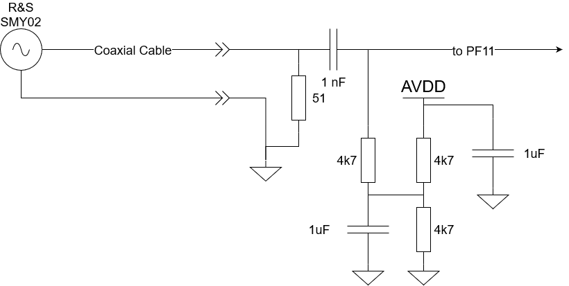
For the single ended input, I used capton foil, copper foil and a SMA edge mount connector, which I directly put on the edge of the NUCLEO board where PF11 is.
This is the circuit diagram:
And here are pictures of the actual board:
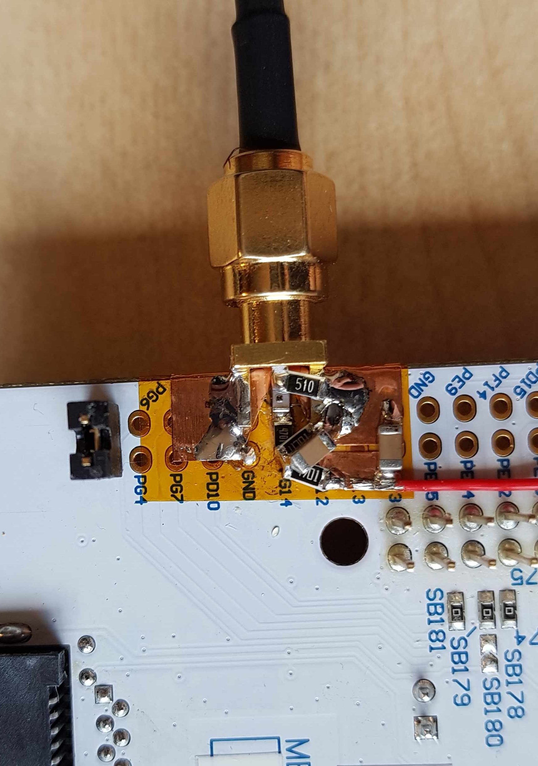
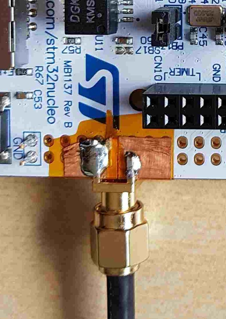
For the differential input, I used a small copper-clad board, size about 2 cm x 2 cm, and drilled three holes in it for mounting the board to the solder pads for GND, PF11 and PF12. In addition, I used a dremel multi-tool for engraving a few traces that facilitate soldering the few components of this circuit:
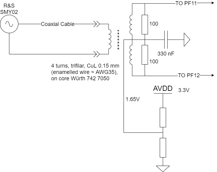
As you read on the schematic diagram, I used a small binocular core for building an unbalanced-to-balanced transformer. Use 3 about 15 cm long pieces of enamelled wire and twist the 3 wires together. Use an Ohm-Meter for finding the correct wires for the center tap.
By the way, one nice features of the transformer is the galvanic isolation between primary side and secondary side. It won’t protect the ADC from a lightning strike, of course, but it will surely give a nice protection against voltages in the tens-of-voltage range.
Here are some pictures of the transformer and the ECB („Engraved Circuit Board“) and how it is mounted on the NUCLEO board. I used 3 pins of an ordinary header for soldering the small board to the NUCLEO board, which gives a quite sturdy connection :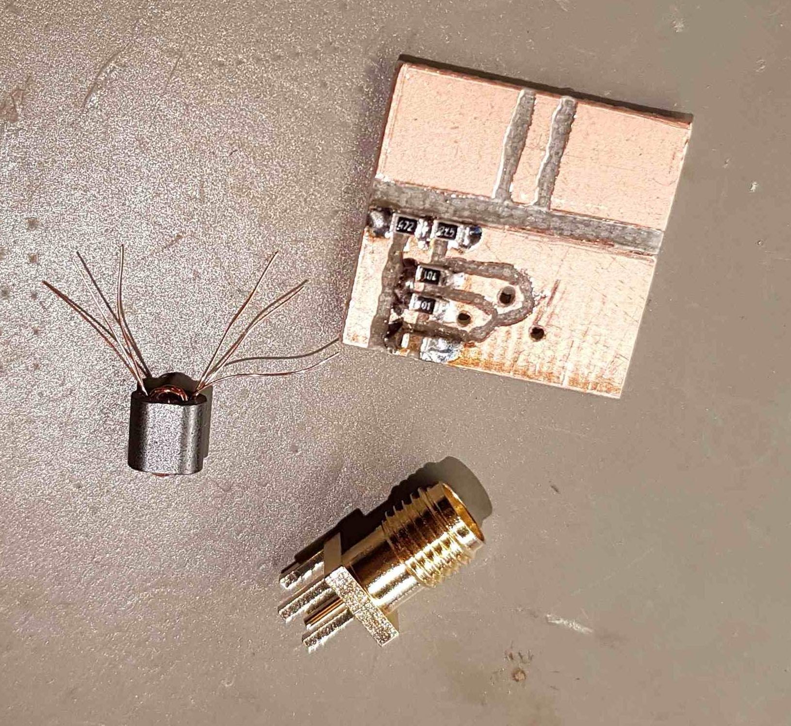
Then I wrote a simple application that puts the ADC into continuous sampling mode. The ADC data are written to a buffer via a circular DMA. Each time the DMA buffer is half full, an interrupt is generated where a flag is set.
Each time the main loop discovers that the DMA-half-complete-flag is set, the first half of the buffer is base64-enoced and written to a transmit-buffer. The transmit-Buffer is then sent out on the Tx pin of the USART3 peripheral.
The code can be downloaded here: https://github.com/papamidas/H7ADCBW
By using STM32CubeIDE, I had to write only a few lines of code. The rest of the application could be configured via the built-in device configuration tool.
I used the following deviations from the reset configuration:
ADC: continuous mode
DAM: DMA1, Stream 0, Circular, Half word, memory increment
USART3: DMA, Normal, Byte, memory increment
RCC (clock configuration): HSE 8 MHz, DIVM2 = /1, DIVN2 = x20, DIVP2 = /8, fracn2 = 0 (this gives an ADC clock of 20 MHz)
Some pitfalls:
If you do not activate the USART3 global interrupt, the DMA-complete-callback-function will never be called!
In my opinion, this is very counter-intuitive and should be changed by ST, but although you will find complaints about that in the web, ST refuses to change this behaviour.
Another pitfall is that you cannot change the location of variables via the device configuration tool. If you just define some global arrays in your code, you won’t be able to send them out via DMA access. The reason for that is that STM32CubeIDE uses the tightly coupled RAM (TCM) as the default location for global variables. Switch on the „build analyzer“ in STM32CubeIDE and you will see what I mean. The memory at location 0x20000000 is fast, it runs without wait states, but it can’t be reached by the ordinary DMA controller. For DMA transfers between memory and USART3, put your transmit buffer into memory region RAM_D2. The DMA controller acts as master of this memory region, and the USART3 peripheral acts as a slave.
Before you can do this, you have to define additional RAM sections in the loader file STM32H743ZITX_FLASH.ld, please have a look.
After this, you can tell the tool chain where certain variables should be located by using some preprocessor macros; please have a look into main.c.
I have no idea why ST does not try to facilitate locating variables and interrupt routines as a feature of their device configuration tool.
In addition, they should also automatically place cache invalidation calls into the DMA callback routines as soon as the data cache gets activated.
In my opinion, one of the very important features of this microcontroller are the memory regions that have different sizes and run on different speeds and the cache controllers that can speed up things enormously in many applications.
It makes a lot of sense to place, for example, interrupt routines in ITCM memory (tightly coupled instruction memory) and certain data in DTCM memory, but there is no support for this task available via the device configuration tool or via the IDE. The same is true for the cache, but here the device configuration tool should also give support on how and when to invalidate a cache. I believe that these features and the lack of support from the documentation and the device configuration tool mean that this product is not being used to its full potential.
…continued in part II
Hello, and thanks for the very interesting and informative investigations into the STM32H7.
I find it annoying that ADC1/2 are so underrepresented in the direct/fast channels on the STM32H7 and that there are no available „fast“ differential pairs (only positive inputs). The datasheet says PF11 and PF13 are fast channels, but you say you used PF11 and PF12 (the latter being considered „slow“).
What kind of issues might be caused by the sampling time asymmetry between the positive/negative inputs of your differential input? It seems this differential sampling was still preferable to the single-ended approach. Which of the single-ended inputs did you use in those tests – the fast (PF11/ADC1_INP2) or slow (PF12/ADC1_INN2)?
Well, it’s been a while ago that I did this, so I don’t remember exactly.
The text and the circuit diagram on page says that I used PF11 as single-ended input.
I have no idea what effects an asymmetry between positive and negative inputs may have; I think the main effect of two slightly different analog input bandwidths is that the differential bandwidth lies between the fast and the slow BW